Heavily based on Projects in Flight's videos attempting to make semiconductor devices at home, our semiconductor research group has spent the last year developing the processes for oxide growth, doping, and photolithography. Over the last few months, we set out to combine our processes and make the simplest semiconductor device there is: a diode.
I will go more in depth about the individual processes we've developed in future blog posts, but for this one we'll stick with a high-level overview and some promising results.
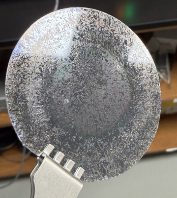
Behold, a diode!
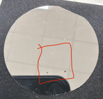
Finished Diode
Our first attempt at a diode was a fairly short process: oxide, lithography, etch, dope, etch. Our process is done on a p-type silicon wafer.
Oxide
Growing a layer of SiO2 on the top of the wafer (referred to as an oxide layer) will allow us to later etch holes into the oxide. This is important because phosphorus (n-type dopant) diffuses easier through silicon than through silicon dioxide.
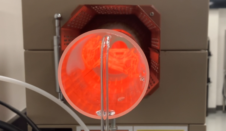 Wafers in the Tube Furnace
Photolithography
Photolithography is the process which lets us create a mask (made of photoresist, essentially UV curable plastic) over the top of the wafer. This mask allows us to selectively etch the silicon dioxide later.
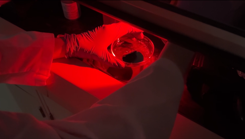 Developing the photoresist
Etch
We use a glass etchant to remove the silicon dioxide that is exposed. Then, we remove the photoresist (as plastic doesn't bode well in a tube furnace).
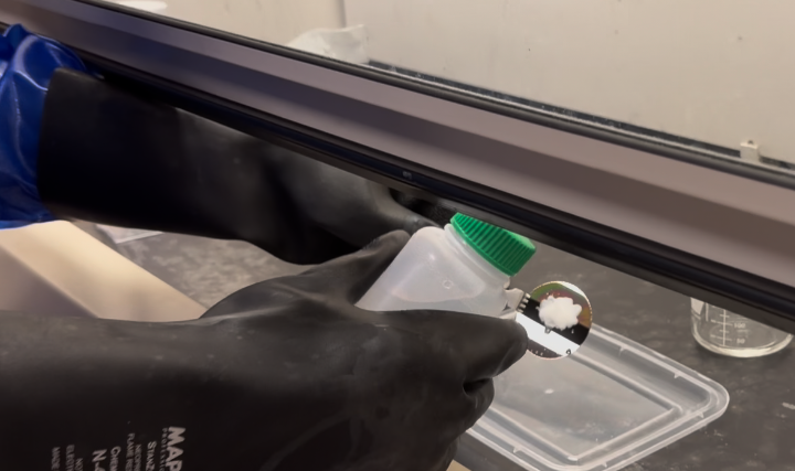 Etching the Oxide Layer
Dope
After spinning on a phosphorus dopant, we drive in the dopant in a tube furnace at 1000C.
The phosphorus dopant after being driven in.
Etch
There's now a new layer of glass from our phosphorus dopant, and we must remove the glass from before putting on the dopant. This is exactly the same as the previous step, but the final product is now an n-well that is exposed.
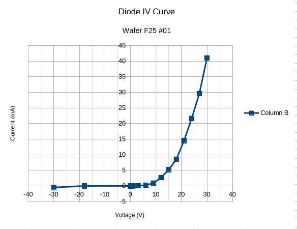
Results
We took manual measurements of our device. This was fairly difficult without metal contacts, as we were basically scraping the top of the silicon wafer to get through the oxide. Wafers are fragile, so this was quite stressful.
Below is the IV (current-voltage) curve of the diode.
 The measured IV curve
The diode appears to have a very large threshold/knee voltage. Further experiments are currently being ran to determine how we can control the electrical properties of the diode.